 In many technical constructions, devices, in laboratory and bench equipment, automobiles used a DC electrical supply voltage of 12 V overload protection, which can lead to spontaneous combustion, is a very important task.
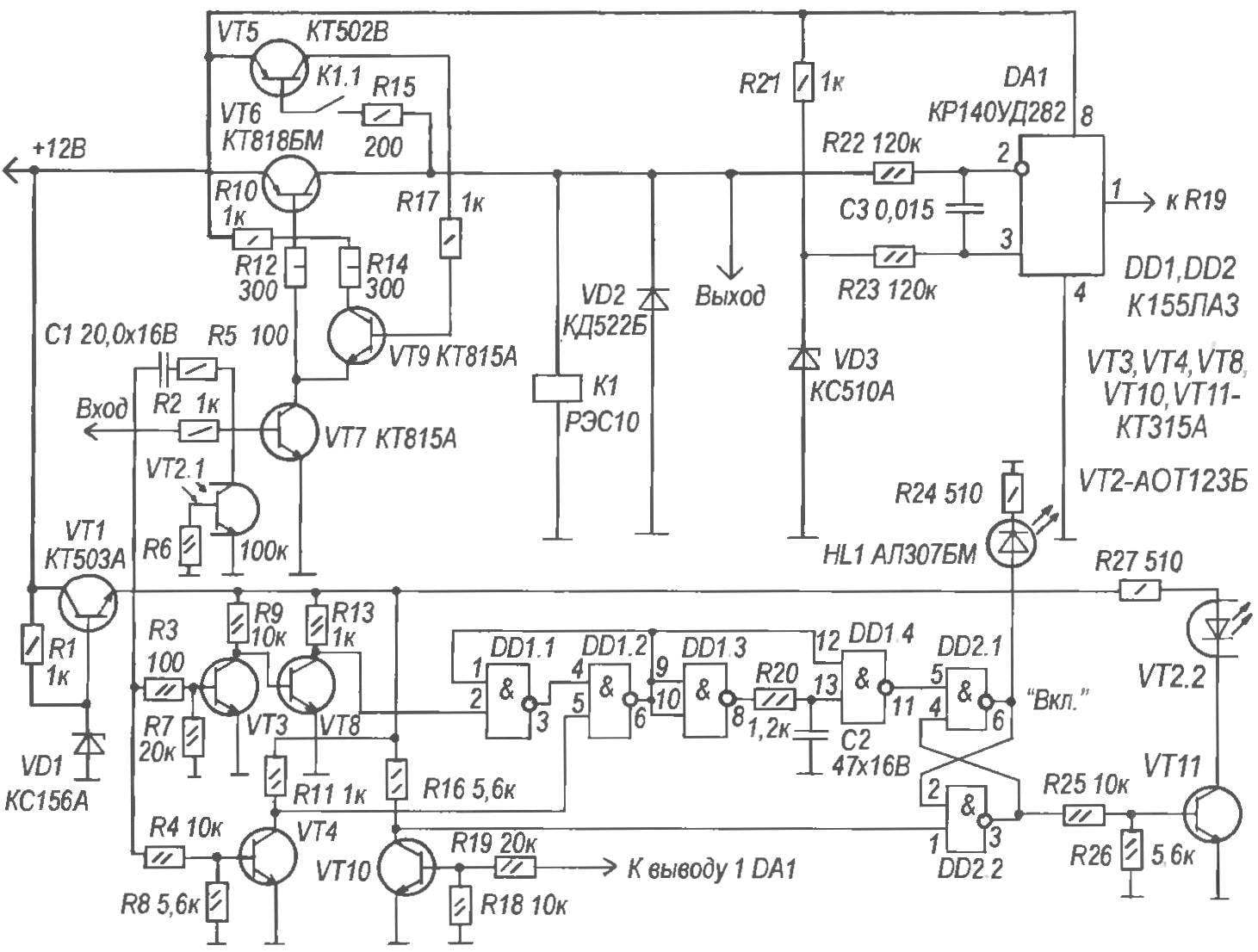
The proposed device is designed specifically for this. It contains: VT6 transistor switch; the control unit of its base current, performed on the transistor VT5, VT9, resistors R14, R15, R17, relay K1; the initial cascade to the transistor VT7, resistors R2, R12; node protection, the Zener diode VD3, capacitor C3, resistors R6, R16, R18, R19, R21 — R23, R25 — R27, the comparator DA1, trigger DD2, transistors VT10, VT11, the optocoupler transistor VT2; node start — on transistors VT3, VT4, VT8, capacitors C1, C2, the resistors R3 — R5, R7 — R9, R11, R13, R20, DD1 chip; a voltage regulator — transistor VT1, the diode VD1, resistor R1, the circuit indication — the led HL1, the resistor R24.
A distinctive feature of this device is the low voltage drop in the open state (which is achieved by the absence of a current sensor for circuit protection), and automatically adjusts the base current of the transistor key (which reduced losses in the control circuit of the key at load currents less than nominal).
The device operates as follows. When the power is connected to the inverting input of the comparator DA1 a voltage is not available, a direct input connected to a reference voltage. The output of the comparator DA1 is set to a high voltage level, the transistor VT10 is opened and the input 1 trigger DD2 is supplied to the low voltage level, and the output 3 is high voltage level; the transistor VT11 open, and led through the coupler VT2 passes current; optocoupler transistor VT2 opens and shunts the transition “base — emitter” of transistor VT7, thereby inhibiting its opening At the output 6 of the trigger is set low voltage level, HL1 led is not lit.
On the chip DD1 assembled shaper of a single pulse of low voltage transistors /TK VТ4, VТ8 — electronic switch. When receiving the input control signal of positive polarity electronic switch is set so that the input 2 of the driver DD1 goes to a high voltage level, and input 5 is low. As a result, the output 11 of the unit DD1 is formed a short pulse of low voltage, whose duration is set by resistor R20 and capacitor C2 and which is fed to the input 5 trigger DD2. The trigger is thrown and the value of voltage levels at its outputs are reversed — the output 3 is low voltage level, and the output 6 is high. As a result, closed VТ11 transistor and the transistor of the coupler VT2. Simultaneously upon receipt of the control signal to the input device via the booster chain C1 — R5 the transistor VT7, and then the transistor VТ6, as a result, the load is connected to the power source. The relay K1 and closes its contacts K1.1, connecting the base of transistor VТ5 the resistor R15. With the increase of the load current occurs, the voltage drop across the emitter-collector key VТ6 to 0.6 volt — VТ5 the transistor and then the transistor VТ9. Resistor R14 is connected in parallel with the resistor R12. The total resistance of the circuit base key VТ6 reduced, the key enters the saturation mode and the voltage drop across it decreases. (This mode of automatic regulation of the base current of the key VT4 prevents false triggering of protection in case of a short-term rise in the load current). At the inverting input of the comparator DA1, you receive the power supply voltage which exceeds the reference voltage supplied to the inverting input of the comparator. It’s output 1 set low voltage level of transistor VT10 is closed. Input 1 trigger DD2 is set to high voltage level. however, this does not affect the trigger condition: at its output 6 is still a high level voltage, and the output 3 is low.

A circuit diagram of a transistor switch with overload protection
In the case of a real overload or short circuit, the voltage at the load resistance decreases to the value smaller the reference voltage set by Zener diode VD3. This leads to the triggering of the comparator DA1; its output level is set to high voltage, the transistor VT10 open, and on input 1 trigger DD2 is fed a low voltage level. The trigger is thrown and the positive voltage level at the output 3 will open the transistor VT11, current through which causes the led of the optocoupler VT2. The last transistor opens and shunts baseemitter the transition of the transistor VT7, which is closed. Is closed and the transistor VT6, disconnecting the power source from the emergency load.
To restore the device to operation after eliminating the cause of overload, you must disable and re-enable control signal of positive polarity to the input of the device, but if you need a manual switch, use the button KME.
The led HL1 confirm the operating status of the device.
The VD2 diode protects key VT6 surge at the moment of disconnection of the inductive load. The stabilizer on the diode VD1, transistor VT1 and resistor R1 at the output has a voltage of +5 volts, for power circuits circuits DD1, DD2 K155LA3 Replacing the diode VD1, it is possible to change the current protection value, for example, when the Zener diode КС133А current is 2.9 A, and the Zener diode КС156А to 2.8 A.
Technical characteristics of the switch:
The voltage, V……………..12
Rated current, a…………………..2
The voltage drop In……………..0,35
Current control, And……………………..0,015
The current protection value, And……..2,5
O. SYDOROVYCH, Lviv
Recommend to read
 AND WILL RELAY SECURITY
Electronic devices and components, in the terminal stages which employ electromagnetic relays, to this day has not lost its relevance among radio Amateurs. Despite competition from...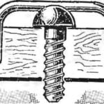 SCREW TIGHTLY
In cases when you want to prevent turning of the screw, screwed into a Board or plywood, I use a very simple way. Of stiff wire or a nail, whose diameter corresponds to the width of the...
