
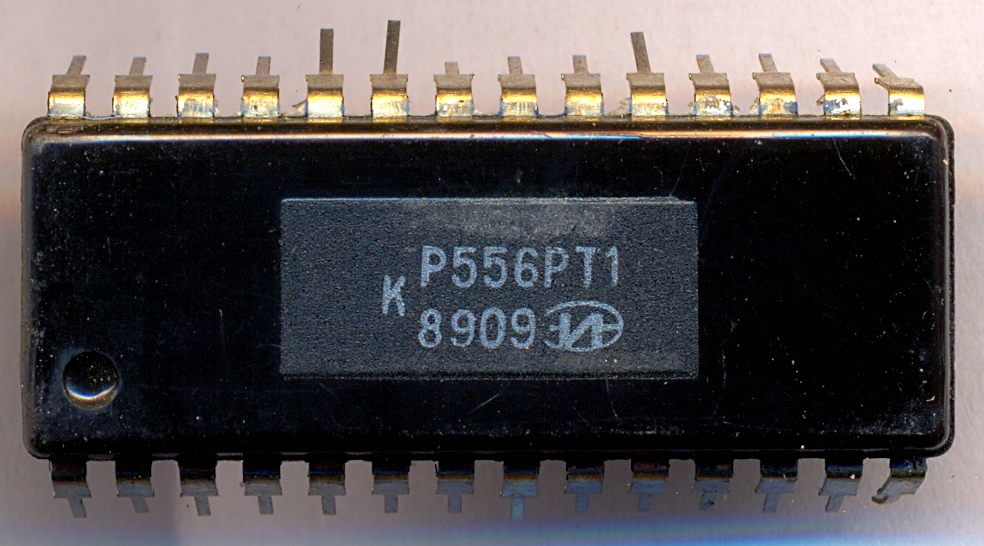
 Hams, self-repairing computers and modern means of automation or manufacturing such equipment, are faced sometimes with the need to record information in the chip programmable logical matrices (PLM). With similar problems they have, for example, to meet when you combine the joystick with the keyboard on the basis of MC КР556РТ1 (КР556РТ2). However, it may be that the existing programmer (even among the so-called universal) are not designed for firmware of these chips. To buy new, more specialized and costly electronic device is not always justified. Another thing is to modify what is already at hand.
A circuit diagram of my proposed upgraded programmer allow minimal cost to solve the problem of “firmware” MC type КР556РТ1 (КР556РТ2). It does not require increasing the number of programmable voltage sources to five as the work-analogues published in several specialized publications. Leveraging technical solutions contained in the existing base unit, it is possible to adapt to work with additional PLM three former source of programmable voltages. Besides, there is no need to complicate an electronic key to transfer them into a state of high output impedance. And this is another advantage of this scheme when compared with other options of improvements of the programmers used for programming logic arrays.
In particular, the matrix “NOT” is programmed by forming alternately on each PLM output of pulses with an amplitude of 17 coming from the voltage log. 1. The latter is supplied to the transistor key VT52 through the diodes VD41 — VD48 (in the log. 1 at the input of the selection of crystal CS inputs ‘ A1 — A16 and a zero voltage PLM).
While the first two timers (the shaper time diagrams) transistors VT25, VT50, VT51, VT52 are open, and the keys КА1—КА16 and КД1—KD8 closed. This interval between pulses of burning. When the third timer appears log.0 bus Q2 authorizing the opening keys КД1—KD8. As a result, the momentum burning.
At all times during the burn matrix “NOT” closed keys K1, KZ, K4, connected to the programmable voltage source E1, E2, E3 (K2, on the contrary, open).
The keys K1 and K2, connected to the output of the programmable voltage source E1, provide a separate supply voltage from the source E1 to the inputs A and b (respectively, through the keys KA and KD). Moreover, it is closed when K1 and K2 is the formation of TTL levels keys KA and KD. Voltage is thus supplied through the diodes VD49, VD50. Since forming In 17 starts during the following pulse burning, thanks to the presence of an output electrolytic capacitor of the source E1 is a smooth increase in the amplitude of the first four pulses of the burn and the tightening of the front fronts of the subsequent pulses. The result is improved accuracy of burn bridges (decreases the likelihood of them “spreading”).
Program burn “OR” forms a voltage E1 = 10, E3 = 8,8, the address code on the inputs of the keys ‘ КА1 — КА6 (outputs Р1С0—Р1С5 port programmer), information about the place burning to the inputs of the data keys КД1—KD8. Bus Q1 comes permission to open key’.
A signal bus Q0, opens the key, assembled on the transistor VT52 and feeding log.1 at the PLM outputs B1—B8. The same happens with the key K4. Opening with the arrival of the signal bus Q4, it then applies voltage Ucc = 8,8 In the output of power PLM.
And on the bus Q2 is supplied permission to open КД1 — KD8. But of these keys opens only one, depending on the location of the log.1 in port Р1В. Open is a wrench fault, causing the voltage of 17 V is supplied to the programming input E of the matrix. But closed the transistor VT50 and, as a consequence, increasing to 10 In the voltage at the terminal CS crystal selection PLM. Removing all of the strain occurs in the reverse order.
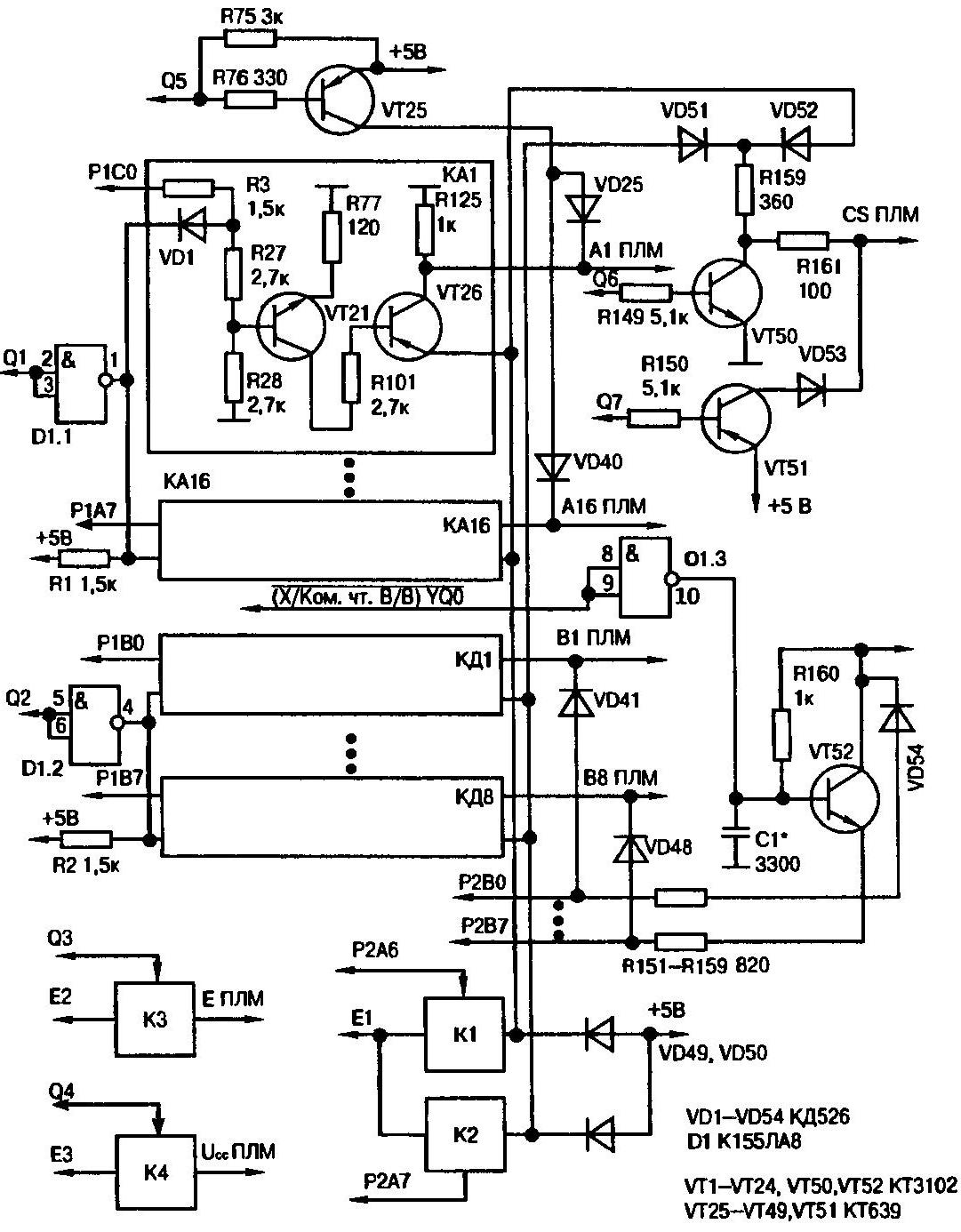
A circuit diagram of a refinement of the most common programmers
Program burn “And” forms E1 = 10ВиЕ3 = 5V. She sets the address code on the inputs of the keys КД1 — КД6 and delivers (via the first ports A and C) information about the place burning to the inputs of the keys of the addresses A1—A16.
The key in forming the pulses of controlled burning in a manner similar to described for matrices “OR”. Fifteen of the sixteen existing PLM inputs receives pulses with an amplitude of 10 V. the only Exception is the entry that defines the place burn. It is served either log.1 for inverse, or log.0 for direct jumper. These logical States are set by key, assembled on the transistor VT25.
During the control information recorded in the matrix “NOT” and “OR” PLM receives the supply voltage is 8.8 V. the Transistor VT50 is opening a VT51 closed. As a result, the CS input crystal selection PLM comes to the state log.0.
Another thing the reading of information from the outputs B1—B8 PLM implemented by the second port (inputs Р2В0—Р2В7). At this time, present signals “X” (this port) and generated by the microprocessor, the read command input-output devices (“Com.Thu.In/in”, according to this wiring diagram). As a result, the transistor VT52 is opened, providing the capability to read information from the outputs B1—B8 (for PLM open collector).
The features of the control information recorded in the matrix “And”. Information retrieval happens with the older release (B8 PLM), while in the younger (B1—B6) is code’. Similarly, the burning of the jumper matrix “And” and in the same sequence served K4 supply voltage 5 V, keys КД1—КД6 sets the address at the outputs B1—B6 (K2 in this case will be closed and current will flow through the diode VD50). The transistor VT25 and keys КА1—КА16 is determined by the place of the reader, and from the VT50 is sent a pulse amplitude of 10 V to the input of the selection of crystal CS PLM. Contrast to burn only in the absence of pulse amplitude In 17, usually supplied by the wrench fault at the input E PLM.
Signals “X” and “Com.Thu.In/in” open a second port for rapid read by the microprocessor information. Them unlocked (but only with a delay, depends on the capacitor C1, the capacity of which is specified experimentally) transistor VT52. This solution, although allows you to read information from the output Q8 PLM open collector, however, distorts the code ‘ set the outputs B1 — B6. However, the microprocessor through the second port To manage it consistently and correctly to perceive even for a short time while the error is still not rise to dangerous levels.
Read matrix “And” perhaps the use of an additional key (same as transistor VT52, but without the timing capacitor). While KD8 must be removed from the key collected in the transistor VT52.
SOLONIN, g. Konotop, Sumy region, Ukraine
Literature
1. Copyright certificate №1654869 USSR, MKI G11C 7/00. Programmer/V. Yu. Solonin//Discoveries, inventions, 1991, No. 21.
2. Click Beetles N. N., Dianov, A. P. programming logic arrays. — Microprocessor tools and systems, 1986, No. 2.
3. Lukyanov D. A. Circuitry universal programmers ROM. — Microprocessor tools and systems, 1985, No. 3.
Recommend to read
 CLEAN — THE GUARANTEE OF QUALITY
A good master always holds his instrument clean. Thoroughly washed with cushion will give a uniform coating of the painted plane, and that it is not collecting dust during storage,... TO CUT THE METAL? EASY!
With sharp sheet metal and non-metallic materials are regularly confronted each homebrew. The use of manual scissors ineffective (especially for large sheets): for large labor, cut...
