
 In technical literature there are many publications on improvised electronic code locks — variety of complexity and management that is performed on chips as small and medium scale integration and microcontrollers. Unfortunately, most of the first it is impossible to quickly change the code, since it is necessary to solder a jumper, or make other changes to the installation. In others, although provides for reprogramming of the microcontroller, but a very limited number of times. Furthermore, these modifiable combination locks consume in standby current of approximately 1 mA, which makes pay attention to the selection of source of energy when you use the above devices in both local (field) conditions where it is impossible to use network adapters.
In particular, look the most attractive at times cheap salt (morganza-zinc) cells from many AA (diameter 14, height 50 mm). Their capacity is in the range from 0.45 to 0.85 And h, and the expected guaranteed duration is 450 — 850 h, or 19 — 35 days. Even more tempting, it would seem that cells of large sizes — alkaline, capacity for AA size is in the range of 1 to 3.7 Ah. But their use of weights and expensive construction, besides not meeting the expectations to radically increase the duration of the lock.
Published below, the device consumes standby current of 40 µa. The operation of this lock is based on the comparison of two binary-coded decimal codes. The first of them is press a button (on keyboard field of ten buttons), the second is stored in ROM. The coincidence of codes, the counter increases his testimony on the unit. In eight matches the output one-shot generates a pulse of high logic level, causing the actuation of the actuator, whereupon the circuit returns to its original state.
The device is working properly in CMOS circuits and “ancient PROM” type hook up, but the food served at the last only the time code reader, which allows you to minimize the power consumption. This provides guaranteed protection of the estimated probability of selection code of the order of 10-8 (100 million combinations).
For comparison assume that for the set one combination of the eight digits required 5 seconds. Then to loop through all the combinations will take 500 million seconds, or more than 15 years. When you add one chip length of the code sequence increases up to 15 digits, making the selection of the code and does the impossible.
Features of the proposed schematics of the castle (Fig.1A) such that in the initial state all counters cleared: DD2 — high level input R (pin 9), a DD4 and DD9 is at power (in this case, the output of the element DD8.4 set the log level.1 for a period of approximately 70 MS determined by the time constant of the chain R16C8). To set the counters to its original state is possible at the push of a button SB11. This is necessary after a failed hitch-hiked to crack a code.
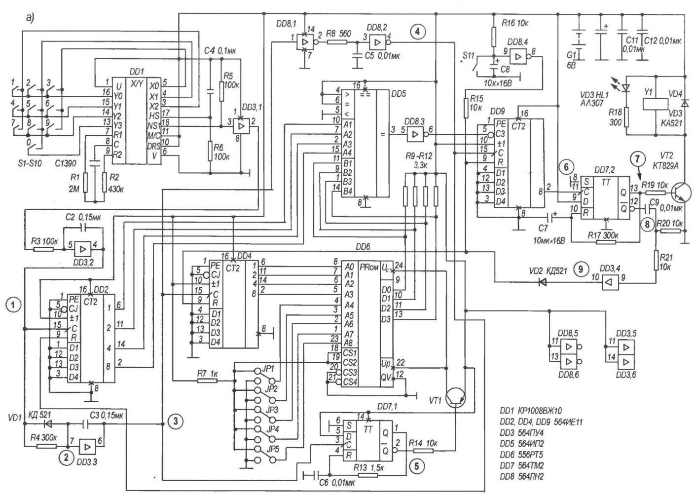
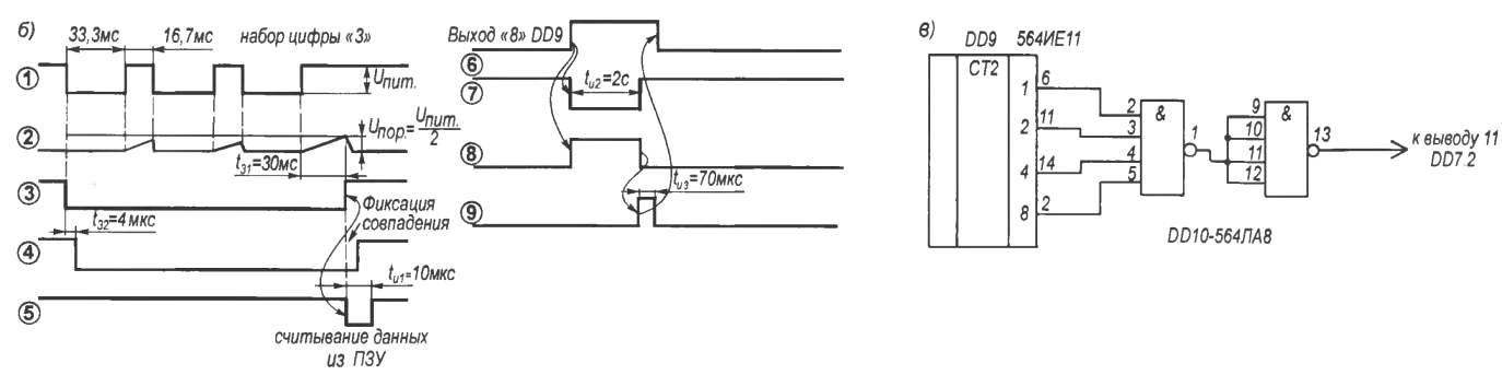
Fig. 1. Circuit diagram homemade programmable code lock (a) plots of the voltages at the test points (b) and the option of its improvement (in)
The input code is generated by means of chip pulse dialer DD1 type КР1008ВЖ10 and binary counter DD2. Connection in accordance with the logic operation (see Fig.1A). HS КР1008ВЖ10 (pin 17) — input from the “toggle switch” (tube); DRS (pin 10) — the frequency selection code of the parcel (10 or 20 pulses per second); input M/s (pin 11) — selects the ratio of the imp./pause (3:2 or 2:1); output NSA (pin 12) output of a spoken key (in this case not used); the output is NSI (pin 18) output switching key. The outputs of the NSI and NSA made on the circuit with open collector.
The repetition frequency of parcels is chosen equal to 20 imp./s (entrance DRS is connected with the “plus” power source), the ratio imp./pause equal to 2:1 (M/s connected with “plus” power source), that is, the length of the parcel log.0 is equal to 33.3 MS, log.1 of-16,7 MS. The output switching key through a pull-up resistor R5 is connected with the “plus” power supply.
When you press any of the buttons in the output switching key, you receive the pulse sequence frequency of 20 Hz with the pulse number corresponding to the pressed button, and an amplitude substantially equal to the supply voltage. Through buffer DD3.1 this sequence is fed to the input shaper consisting of DD3.2, R3, C2. Chain R6С4 is used for the initial installation of the chip dialer at power-up.
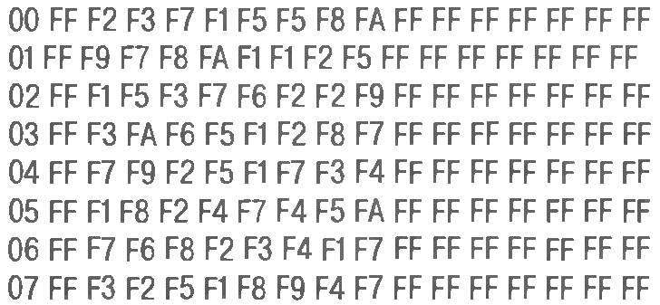
Example firmware code ROM (fragment)
The driver has the properties of a Schmitt trigger and an integrating chain. Pulses at its output (Fig.1B, figure 1) have steep fronts, regardless of the steepness of the input pulses. In addition, it suppresses impulse noise of short duration, as the capacitor fails to charge to the switching threshold of logic element DD3.2.
With the shaper’s output pulses are applied to the detector packages, which is collected on DD3.3, VD1, R4, C3, and operates as follows. The first negative pulse sequence passing through the diode VD1 to the input of the cell DD3.3, switch it in the log.0. In the pauses between adjacent pulses of the sequence, the capacitor C3 is charged through the resistor R4, however, the input voltage DD3.3 does not reach the switching threshold.
Each subsequent pulse, quickly discharges through the diode VD1, the capacitor C3 (Fig. 16, schedule 2) so that during the passage of the sequence at the output of the cell DD3.3 will log.0. In the pauses between sequences of the voltage on the capacitor C3 reaches the threshold switching, and the above cell is put in the log.1. This happens in approximately 30 MS after the end of the set. Thus, during the pulses when dialing any digits at the output of the detector packages is high.0.
Simultaneously, the pulses output from the driver arrive at the counting input of the binary counter DD2. This chip counts the number of pulses (the account is based on positive slope) and remembers it.
The outputs DD2 there is a binary code the number of pulses. This code is supplied to one of the ports of the digital comparator DD5 (inputs A1 to A4). A positive voltage is supplied at the end of the numbers on the counting input of the binary counter DD4 and sets its outputs code 0001.
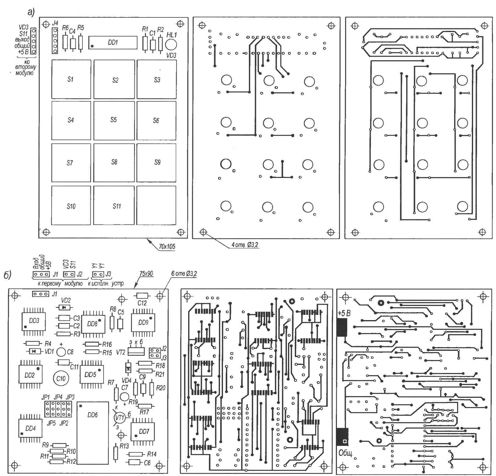
Fig. 3. The topology of double-sided printed circuit boards of the first (a) and second (b) modules code lock
This code is supplied to the insignificant bits of the address bus of the ROM chips DD6. Code high-order bits of the address bus is formed by removable jumpers (jumpers) JP1 — JP5. Thus, the possible 25 = 32 code combinations.
Simultaneously, the positive voltage fed to the input of one-shot consisting of D-flip-flop DD7.1 and elements C6, R13. This difference in the inverse of the trigger output there is a short negative pulse (Fig. 16, graph 5) with a duration of about 10 µs. This pulse is fed through a current limiting resistor R14 to the base of transistor VT1 and opens it.
Through the open transistor VT1 provides power to the ROM chip DD6, and at its outputs D0 — D3 appears the binary code contained in the cell with the number 0001. This code is supplied to the second port of the digital comparator (inputs B1 — B4).
Compares the code contained in ROM code and the output of the counter DD2. When they coincide (that is, when you set the “correct” numbers) at the output of digital comparator DD5 (pin 3) level appears log.1, which is inverted logical cell DD8.3. Log.0 from the output of the latter is applied to inverted carry-in input CJ of the binary counter DD9, allowing the account.
On the counting input of the counter DD9 receives a delayed signal from the output of the shaper (Fig.1B, schedule 4). Delay circuit elements is DD8.1, DD8.2, R8, C5 and has a value of about 4 µs. During this time, data is read from the ROM, there is a comparison of codes and a low logic level at the input CJ of the counter DD9. The coincidence codes counter DD9 increases his testimony on the unit.
If the codes do not match, the output of the digital comparator is present in the log level.0, at the input CJ of the counter DD9 — log.1 (which prohibits the account), and a positive differential at its counting input causes no variation in the readings.
From the output of the inverter DD8.2 the signal supplied to the reset input of the counter DD2. The appearance of the log.1 at the entrance To the DD2 counter is reset to zero, after which it is ready to receive a new pulse sequence (following figures). When you set the eight “correct” digits in the output “8” of the counter DD9 (conclusion 2) there is a positive difference (Fig. 16, figure 6), which is received by the single vibrator, consisting of a trigger DD7.2 and elements R17, C7. This drop triggers the one-shot, and direct the trigger output appears a positive pulse of about 2 s (Fig. 16, figure 7).
The latter opens up the composite transistor VT2, which connects the actuator to the common wire. Led HL1 indicates the inclusion of the actuator. At the same time on the inverse trigger output DD7.2 there is a negative pulse of the same duration (Fig. 16, chart 8), the trailing edge of which elements C9, R20 and R21 are forming a positive pulse with a duration of about 70 MS, which via the buffer DD3.4 and the diode VD2 is supplied to the inputs R of counters DD4 and DD9, resetting them. Thus, the scheme is set to its initial state and becomes ready to receive the next codeword.
An example excerpt of a firmware ROM is provided (Fig.2). You can use their invented codes, only when it is necessary to consider that the dialed digit “0” (chip DD1 produces 10 pulses) corresponds to A code (1010) ROM. One line of the listing corresponds to a single code. The actual code starts with addresses 01, 11, 21, 31, etc., ending, respectively, on address 08, 18, 28, 38.
Senior nibble of memory cells not being used, so it is possible to write code F (chip КР556РТ5 in the initial state “protection” log.1). Thus, the first line of the listing corresponds to code 23715580.
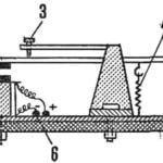
Structurally, the combination lock is made of two modules (on a bilateral printed circuit Board) and the Executive device. The first module (Fig. 3A) contains a keyboard S1 — S11, the dialer chip of DD1, timing elements R1, R2, C1, the circuit for initial installation R6С4 and pull the resistor R5 and the led. HL1 is mounted to the external side of the door and connected by flexible wires with another module that has other parts, except the actuator, which is a low-power solenoid: that only removes the lock, and pulls the lock bolt.
Unused inputs of logic elements connected to the “plus” of the power source. Capacitors C10 — C12 (Fig. 3b) is blocking.
To increase the secrecy of the lock you can increase the number of digits in the code. This requires insights 2,6,11, and 14 of the counter DD9 (Fig.1B) connect to the inputs of logic cells 4I, and the output of the last — to the counting input of the trigger DD7.2. You can use the chip К564ЛА8 (2 the element 4I-NOT) and included the second cell inverter. In this case, output one-shot start after the 15th match.
As the power supply uses 4 cells total voltage of 6 V. They are mounted with a steel bracket on the back side of the second module. The operability of the lock is preserved when reducing the supply voltage to 4.8 V. of Course, you can use network and power sources, and as actuators to apply a low voltage relay that controls the 220-volt solenoid, which will pull the lock bolt. However, in the absence of mains voltage the access to the room will be impossible.
The device uses chip series 564 (DD2 — DD5, DD7 — DD9), КР1008ВЖ10 (DD1), КР556РТ5 (DD6), КТ3107К transistors (VT1), KT829A (VT2), resistors-2-22 with a power dissipation of 0.125 W, condensers KM-5 (C1), KM-6 (C2 — C6, C9, C11, C12), K50-35 (C7, C8, C10), diodes KD521 (VD1 — VD3), led АЛ307 (HL1). As buttons SB1—SB11 can be used almost any suitable, are not fixed. In the author’s version of them — from the computer keyboard. As the jumpers jumpers are used, similar to that used in computer circuit boards, whereby the lock code can be changed in just a few seconds.
Instead of chip series 564 you can use the IC series 561, however, this will increase the dimensions of the second module and will require a change in the topology of the PCB. As elements of power it is better to use alkaline battery cells.
V. VASILENKO, Sverdlovsk, Luhansk region, Ukraine
Recommend to read
 ELECTRIC SAW
This simple saw can be processed plywood, thin wooden boards, etc. On the basis of the size of 250X150 mm are mounted the following parts: 1 — the solenoid of the screw Ø10 mm, which is... AND SIMPLY AND CONVENIENTLY
Lee leaves baby stroller out of the house (where now find entrance without stairs?), overcome whether the underpass is on the platform of the station or stations everywhere have to...
