 The formation of ice on the surface of the blades of the rotor (screw) microgenerator-ROV, wind turbines, anemometers, propeller vanes, fans, degrades performance and may lead to dangerous modes of operation – imbalance, vibration, destruction of bearings, the possibility of destruction of the structural elements is relieved by ice. To prevent such operation it is necessary to detect and eliminate incipient icing.
The proposed indicator can serve as a basis protivoallergennye-tional system of such devices. Its principle of operation is based on polarization-optical method for remote monitoring of the presence of ice [1], which provides high sensitivity and speed. In its technical essence is the device closest to the signaller icing of the propeller blades of the helicopter [2], pomekhoustoichivost.
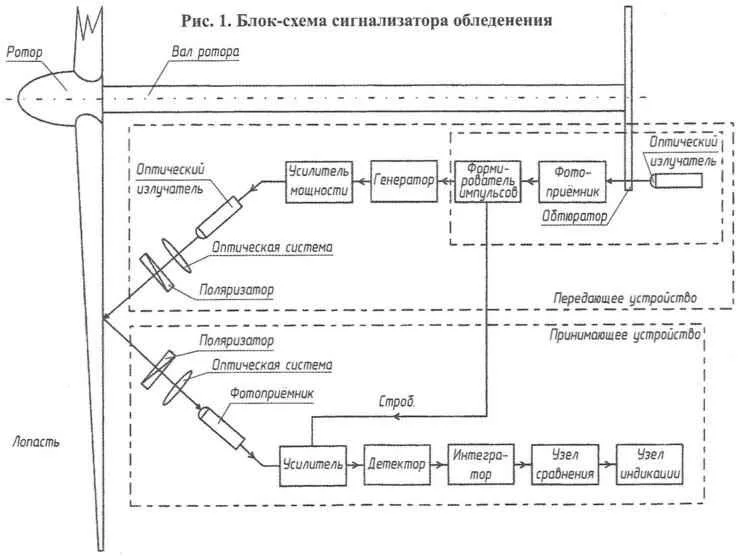
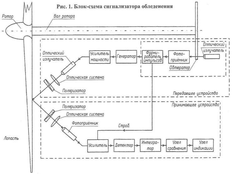
The block diagram of the alarm device shown in Fig. 1. It consists of transmitting and receiving devices. The transmitting device comprises a synchronization host, generator, power amplifier, optical transmitter, optical system and a polarizer. The node of the synchronization includes the obturator, an optical emitter, the photodetector and the pulse shaper.
The shutter is an impeller mounted on a shaft of the rotor, number of blades which is equal to the number of rotor blades and their chord equal to the chord of the rotor blades in the control zone. The spatial orientation of the impeller blades of the obturator relative to the axis of rotation of the rotor shaft coincides with the orientation of the blades of the rotor.
The receiver consists of a polarizer, optical system, photodetector, amplifier, detector, integrator, host comparisons and site indication.
Seal due to axial rotation of the rotor shaft periodically blocks the beam of the optical emitter node synchronization, modulating the amplitude of the output signal of its photodetector. Electric signal output from the photodetector node synchronization to an input of a pulse shaper, which generates from it the rectangular pulses of fixed amplitude, the duration of which is equal to the time interrupt optical communication between the emitter and sensor node synchronization.
Node synchronization through pulse shaper controls the operation of the transmitting and receiving devices of the alarm device so that radiation of the transmitting unit occurred only in those moments of time when a rotor blade intersects its optical axis. In these moments, the gain of the amplifier of a receiving device is maximum. At other times the sending device does not emit, and the gain of the amplifier of the receiver is minimal.
When the rotor arm crosses the optical axis of the transmitting device, the output of the generator is formed by a sequence of rectangular pulses, which through the power amplifier modulates the amplitude of its radiation. This radiation passes through an optical system forming the beam with a small divergence angle, and polarizer that transmits only those waves, the polarization plane of which coincides with its plane of polarization.
Polarized beam reaches the surface of the rotor blades and being reflected from it, gets to the entrance of the receptor. In the receiving device the beam is a polarizer, the plane of polarization which is turned by the angle providing the minimum level of passing through it of the reflected optical radiation. This radiation is focused by the optical system receiving device on the sensing element of the photodetector, which converts it into an electrical signal. Electric signal output from the photodetector, passing successively through functional units of a receiver, amplified, detected, integrated and analyzed at the amplitude node of the comparison, control operation of the display unit.
If there is icing of the rotor blades, the beam reflected from the ice layer depolarized. The reflected waves whose plane of polarization coincides with the plane of polarization of the polarizer located in the receiving device, pass through it freely, so that the amplitude of the electrical signal at the output of the photodetector increases, and the display unit of the receiving device generates a warning signal about the presence of icing.
The elimination of natural or forced through a layer of ice from the surface of the rotor blade stops the depolarization of reflected beam, whereby an electrical signal at the output of the photodetector is reduced to the initial level. The display unit of the receiving device generates a warning signal about the lack of icing.
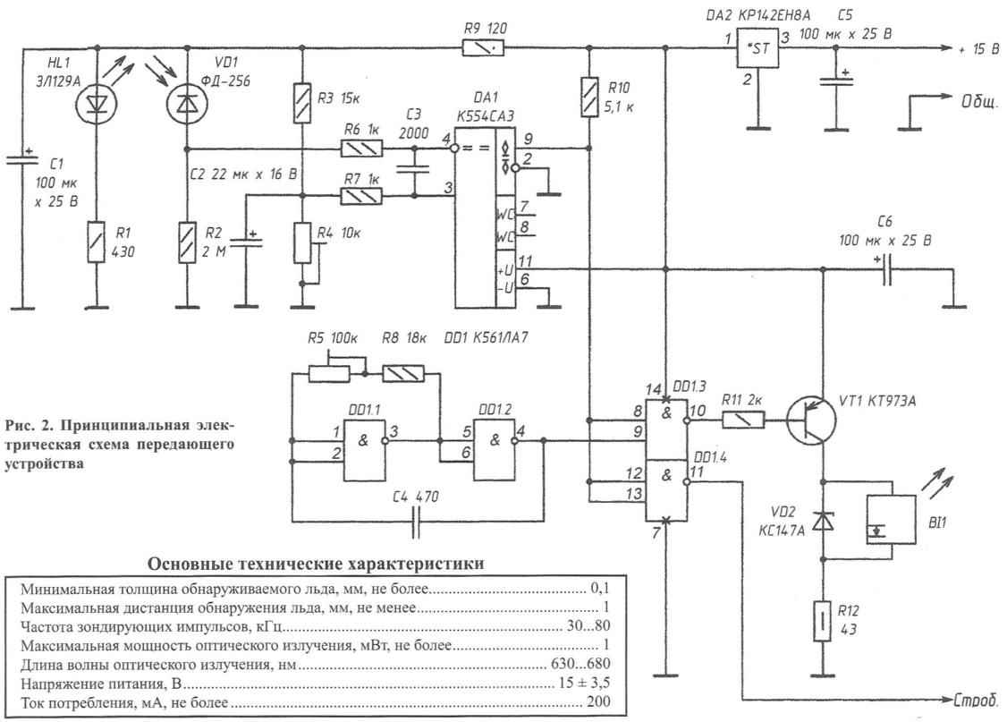
Fig. 2. A circuit diagram of a transmitting device
A circuit diagram of a transmitting device shown in Fig. 2. Optical emitter node synchronization is performed on the HL1 led, working current which is set by resistor R1. The sensor node synchronization is a photodiode VD1, the load which is a resistor R2. DА1 chip, logic element DD1.3, resistors R3, R4, R6, R7, R10 and capacitors C2, Sz form a pulse generator. Capacitors C1, C2 and resistor R9 – items-filtering the synchronization host.
The generator includes logic elements DD1.1 – DD1.3, resistors (R5, R8 and capacitor C4. The amplifier formed by the transistor VT1, a current-limiting resistors R11, R12 and Zener diode VD2. Optical emitter transmitting device-a semiconductor laser BI1. Zener diode VD2 protects the semiconductor laser ВІ1 from excessive voltage. The transmitting device is powered by a voltage regulator implemented on a chip of DA2 and the capacitors C5, C6.
A circuit diagram of a receiving device shown in Fig. 3. Adopted optical radiation is converted into an electrical signal by photodiode VD1. Amplifier receiver made on microcircuits DA1, DA2, resistors R1 – R14 and capacitors C1 – C4. The voltage divider R1, R12, resistors R2, R7, R10, R14 provide for the operation of the circuits DA1, DA2 DC. Resistors R3 – R5 and capacitor Sz form a chain of negative feedback (NFB) of the first amplifier stage. The circuit is OOS of the second stage of the amplifier consists of a resistor R9, channel field-effect transistor VT1 and resistor R13. Resistors R6, R8 and R11 provide a mode of operation of the DC bipolar VT2 VT1 and the field effect transistors, respectively. Capacitors C2, C4 separation. The amplifier is powered by voltage regulator, implemented on the chip DA3. Capacitors C1, C6, C9 – filter.
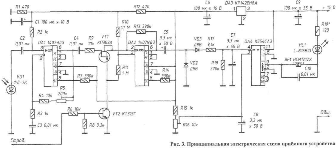
Fig. 3. A circuit diagram of a receiving device
At a low logical level Stro-berousek pulse coming from the corresponding output of the transmitting device, a bipolar transistor UT2 is closed and the field effect transistor VT1 is open, the gain of the amplifier is maximum. With the appearance of a high logic level straberry-present pulse of the bipolar transistor VT2 is opened, and the field effect transistor VT1 is closed, the gain of the amplifier is minimal.
The detector and integrator include diodes VD2, VD3, capacitors C5, C7 and resistors R17, R18. The comparison unit is a voltage comparator implemented on-chip DА4. The voltage divider R15, R16 sets the threshold trigger voltage of the comparison unit. Capacitor C8 is a filter.
The display unit consists of a flashing led НL1, resistor R19, capacitor C10 and the emitter of the sound ВF1. If the icing is not detected, the led НL1 off and the transmitter of sound ВF1 not working. When it detects icing НL1 led starts blinking and the transmitter of sound ВF1 intermittently sound.
The details of transmitting and receiving devices of the alarm device mounted in hinged manner on the breadboard.
As polarizers transmitting and receiving devices used polarizing filter from DMM with LCD readout. In the receiving device provides the possibility of circular rotation of the polarizer in the polarization plane.
Optical emitter transmitting device is a laser pointer, equipped with insights to enable connection to the electronic unit. On it borrowed optical system of the transmitting device. The optical system receiving device is a small mobile lens.
The indicator used oxide type capacitors K53-35, but it is permissible to apply similar import. Ceramic capacitors K10-176 (or KM-3 KM-6). Fixed resistors – C2-33 (can be replaced by C2-23, MLT, OMLT). Podster-ecznie resistors – CP3-39 (or JS3-37, RP1-48).
Д9В diodes can be replaced with diodes of the same series with an alphabetical index G – L or germanium diodes other series, for example: D2, D10, D18, D20, Д310 – Д312, ГД107, ГД402, ГД507. Zener КС147А permissible to replace the Zener 2С147А. Led ЗЛ129А replace LEDs series AL 107, ЗЛ107, АП118А, ЗЛ118А. Photodiode FD-7K is acceptable to replace the photodiodes FD-17K, FD-18K, FD-24K. Photodiode FD-256 can be replaced by photodiodes FD-21КП, FD 25K, FD-26К. Instead of flashing the led L-816В1D permissible to use any the same, for example, L-796В1D.
Chip K561LA7 can be replaced by any functional equivalent from domestic or imported series of ICS in CMOS structure, for example, 564ЛА7, К176ЛА7 or CD4011. Chip 1407УДЗ permissible to replace the analogue from К1407 or imported – EC-41. Chip К554САЗ can be replaced by a chip 521САЗ or imported LM311. Chip КР142ЕН8А interchangeable branded analogue series 1509.
Instead of the transistor КТ973А you can use the transistor КТ973Б or imported BD876. KSOZE transistor can be replaced by transistors of the same series with an alphabetical index, W or transistors KP307 with letter indices A – E. the Transistor КТ315Г permissible to replace any equivalent transistor, for example, a series КТ342. Elektromagnetic НСМ1212Х possible to replace the emitter НСМ1612Х.
The establishment of the transmitting device of the alarm device is to install a trimmer resistors R4 and R5 (Fig. 2) the response voltage of the pulse shaper and the working frequency of the generator, respectively. The working frequency of the generator should be installed within the bandwidth of the amplifier receiver. In the presence of a radiation transmitting device make sure. The sensitivity of the alarm adjust trimmer resistors R15 and R16 (Fig. 3) that sets the gain of the amplifier and the threshold comparison unit, respectively. Flashing mode led HL1 (Fig. 3) is achieved by selection of resistor R19.
During configuration of the alarm device the ice can be simulated cellophane or plastic wrap, placing it on the surface of the test object. The final regulation of the signalling device are produced in real icing by orienting the transmitting and receiving device relative to the surface of the blades of the controlled object, and the polarizer receptor – relative to the polarizer transmission device so that in the absence of icing, the amplitude of the signal at the output of op-amp DА2 (Fig. 3) was minimal, if any — max. High achieve also a change in the focal length of the optical system of the receptor.
It should be noted that the above-described alarm device suitable for monitoring icing of the blades, made of electrically conductive material. If the blades are made of dielectric material, polarizing the reflected beam, in a controlled area necessary to ensure their continuity, for example, securing the blade strips of thin aluminum foil. When working with the indicator avoid contact with direct or reflected laser beam directly into the eye.
O. ILYIN, g. K a z a n
Recommend to read
 BRITISH TWENTIES
The development of the project tanks for the British army in the early 1920s was run by the company "Vickers" — England's largest manufacturer of weapons and armored vehicles. The new...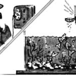 FEEDING BY… PHONE
Aquarists are often literally confined to the house: indeed, even for a few days can't leave the fish without food. Meanwhile, feed the fish and you can remotely, via an ordinary house...
