DESIGN THE PRINTED CIRCUIT BOARD

PCB DESIGNNovice hams are often hesitant to begin the Assembly of electronic devices just because in the description is missing the picture of the PCB, and to develop its own not everyone can. Indeed, without sufficient experience to make it easy: it is necessary to know how to choose the best dimensions to correctly place items in a timely manner to detect and correct errors. Therefore, we recommend you to master the design of printed circuit boards with the simplest.
The Board size and the location of the printed conductors depend on the number of set a elements and their types, why not get to work, making sure that prepared all the necessary radio components. Pick them in accordance with the concept and description of the instrument and is also considering possible replacements. First of all you need to choose the right types of capacitors: it is important not only capacitance and working voltage that they are designed, but their frequency properties and qualities of the dielectric. If, for example, in the radio frequency device to apply capacitors on the basis of low-frequency ceramic or paper (MBM, BM-2, etc.), it can be generally unworkable.
 
Fig. 1. How to install radio elements on the circuit Board
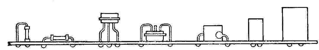
Fig. 1. The methods of installation of radioelements on PCB
 
Between mounted on printed circuit Board elements often have complex reciprocal relationships. Their influence could weaken the positioning elements based on the principle of their action and increasing the distance between them. Therefore, you should not strive for reduction of fees due to seal installation. Close the installation may deteriorate and the thermal design of electronic device that interferes with his normal work. In the radio frequency devices is not unnecessarily lengthen the connecting conductors, to arrange the elements of the individual stages in close proximity to each other to be placed close to the input and output circuits.
 
Fig. 2. Application of radioelements
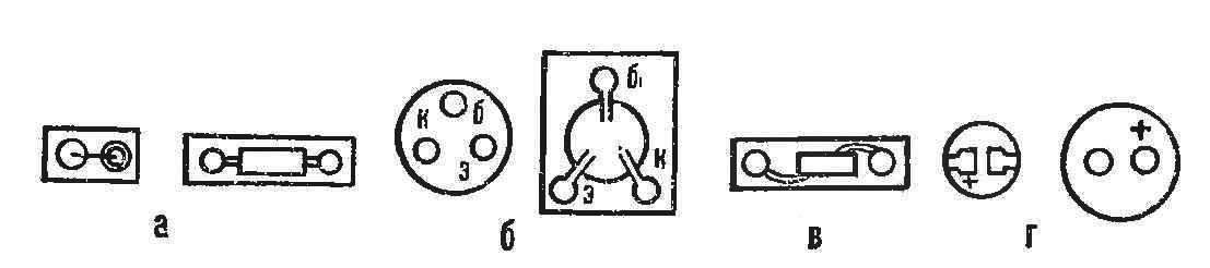
Fig. 2. Application of the radioactive elements:
a — resistors MLT, b — low power transistors, a capacitor, KM-5, g — condenser K50-6.
 
Perhaps the greatest difficulties encountered in the development of printed circuit boards amplifiers and oscillators, and increase the operating frequency, gain, number of stages, as well as capacity increase, with increase of requirements to stability of frequency and voltage generated by the task becomes more complicated. The easiest way to develop printed circuit boards for power supplies — just enough to ensure the normal thermal regime elements and, of course, to avoid mistakes. By the way, the errors to the drawing boards need to be identified at all stages of development: the earlier they are detected, the easier it is to fix them.
 
Hams used both one-sided and double-sided printed circuit Board. Beginners recommend only one-sided. All the radioactive elements in them are on the one hand, and connecting the terminals elements printed conductors on the other.
 
The methods of installation of components on the Board can be different (Fig. 1). The findings of each of them into the desired shape — curve, to give them a certain configuration, and the location of bends and distance from body to soldering shall conform to the conditions of this element, details of which can be found in the handbooks.
 
So, transistors can bend the findings are not closer than 2 mm from the body, in turn, the bending radius depends on the diameter of the output than it is thicker, the smaller the allowable curvature. Insights powerful transistors (КТ803, КТ805 and the like), bending is impossible, and semiconductors with the findings of shorter than 10 mm for novice hams better not to use.
 
The order of placing the electronic components on the PCB is called a layout. From it largely depends on the performance of the electronic device. For example, bad layout of the circuit Board of the generator may cause it unstable, and the radio frequency amplifier to cause self-excitation.
 
Fig. 3. Schematic diagram of amplifier
Fig. 3. Schematic diagram of the amplifier
 
Use the application, image, model and field methods of layout. For beginners the first most acceptable. Within the future Board of optimally placed of an application (Fig. 2) pieces of thick paper, which depicts the contours of the radioactive elements with the method of installation and the forming of conclusions. The elements thus represent a little more than natural, thereby contributing to the reduction of mutual relations and improving thermal mode of the device.
 
In addition to the circuits of radio, on the applications indicate contact pads for connection of leads (in the form of circles d 2.5 mm) RefDes on the schematic diagram (e.g., VТI, R4, C2), the names of the insights of semiconductor devices, the polarity of the inclusion of electrolytic capacitors, etc.
 
The distance between the images of contact pads should not be less than 1 mm. the drawing is done on drawing paper with ink or ball-point pen, reference designators and number of connection points (about them later), it is recommended to put down a pencil that will allow you to use the application repeatedly by erasing the labels and replacing them with new ones. On the back of the picture indicate the specific types of elements to which it corresponds (e.g., МП16, МП26, МП39, МП42). Thus create a set of applications and then use them when designing printed circuit boards.
 
P and P. 4. Placement of appliques.
R and S. 4. Accommodation applications.
 
Recorded and connectivity charges with other units, power supplies, elements of switching, adjustment and indication belonging to the design. It is also important to choose how to arrange the Board in the case of the apparatus — either vertically or horizontally, to determine the number and location of attachment points, as well as their design (stand, tripod, bracket, etc.). For them and elements of the external connections necessary to plan in advance the places on the Board, free of radioactive elements and contact pads.
 
Before starting a layout work will redraw the circuit diagram on a separate sheet of paper and number all the points of connections of elements and the external relations Board. Picking up the application, fill in the corresponding circles the numbers of the points, and the contours of the radioactive elements — their reference designators. It is useful to make a sign indicating the number of times each of the connection points found on the applications. It will help to monitor the progress of the preparation of drawing boards and avoid gross errors.
 
On a sheet of graph paper, draw two lines mutually indicate instead. The point of intersection determines the position of one of the corners of the future Board. With him and start the layout of the applications, trying to place them so that the same pin numbers of the elements were as close to each other, and the image of the passive elements of the cascades tended to the respective transistors. Cope that the pads were not in the vicinity of sites to be occupied by the attachment.
 
As a result, all of an application have approximately the same density to be accommodated within the rectangle, pads for external connections to be on the edges of the Board, and pads for connecting input and output wires is at a maximum distance from each other. After this, snap the circuit Board after the missing lines of the sides of the rectangle.
 
Post each application on the selected place with rubber glue, apply to the drawing sheet of tracing paper and transfer it to the Board outline of the PCB and the contact pads. On the images of the mark elements of their reference designators, on the pads of their numbers. Now you can start to develop a pattern of printed conductors. To do this, use the front side of the drawing on the tracing paper (side view of set elements).
 
Connect alternately thin pencil lines all pads with the same numbers referring to the table. The course of select lines such that each of them can be extended up to 1 mm when the gap between adjacent lines of not less than 1 mm. If in a circuit the flow of large currents, the width of the respective conductors should be increased to 2-3 mm. it May happen that the conductors intersect. In this case, you will have a line break and ends, located on both sides of the crossing lines to depict additional pads with the number of broken lines During installation they must be connected with a jumper wire, and while it should be depicted as a dotted line labeled “per.”.
 
Flip the sheet of tracing paper the reverse side (seen from the printed conductors), draw alternately, guided by the thin lines, all printed conductors with a width of 1 mm, maintaining the same gap between adjacent conductors and pads. (Width of the conductor, which is connected to the “grounded” terminal of the power source should be more.) You will receive a drawing of the Board with constant width conductors. It can be modified to other flavor — with a constant gap between the conductors. Board with the same pattern are widely used in the manufacture of factory and Amateur radio devices, it is usually due to vacant seats between the other conductors maximizes the area occupied by “grounding” conductor. The advantages of these boards — more efficient common wire, better shielding elements and a significant savings of the solution during etching.
 
Fig. 5. PCB uzch
Fig. 5. PCB uzch
 
Tracing — material fragile, so the pattern of printed conductors should be transferred to a sheet of heavy paper. In addition to the conductors with the centers of the future holes for findings of the elements in this figure indicate holes for fastening the Board and the bulky shapes of the clippings (if available). This is an auxiliary figure for direct work with a blank of foil material (see article “How to make PCB”, “M-K” No. 11 in 1985). An original, executed on tracing paper, use as a guide when installing the elements on the manufactured printed Board.
 
Consider as an example the procedure for the development Board for mounting the power amplifier of audio frequencies. The device used low-power transistors 6, 10 fixed resistors, one semiconductor diode, 5 capacitors and 2 electrolytic capacitor of other types. Choose the capacitors C50-6 KLS (C7) and BM-1 (C8).
 
Schematic diagram of the amplifier and maintain the same notation and the numbered connection points of the elements shown in figure 3. The location of the appliques and the pattern of printed conductors are depicted respectively in figures 4 and 5. Because of the small distances between terminals of electrolytic capacitors (2.5 mm) form contact pads for them to change.
 
Board sizes can be reduced if the resistor is mounted vertically and the elements to place tighter. In this case it is acceptable, since the amplifier no large voltages and currents, and the ratio of its gain is small
 
V. Knyazkin

Recommend to read

  • SEAPLANE W-2SEAPLANE W-2
    SEAPLANE W-2. Scale model 1:33. In Russia in the late 20-ies of the last century there was an urgent need in small aircraft for communication with remote facilities. Especially this...
  • STEEL “HEATER”STEEL “HEATER”
    This stove I installed in the bath at their summer cottage. For ten years I use it and is very happy. The furnace body of metal, is welded from a steel sheet with a thickness of 5 mm....