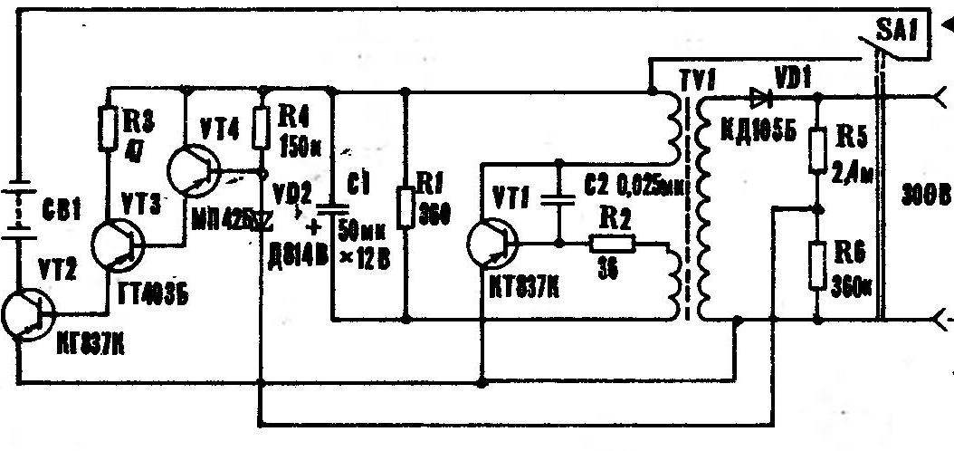
As a stand-alone power source flash FIL-46 I use a voltage Converter PN-70, manufactured by Kharkiv enterprises “ECHO”. In the process of operation of this device revealed its drawback: after charging the storage capacitor and ignition indicator lights, signaling willingness to work consumed by the inverter current decreases from 1.5 A to About 1 A, that is, the batteries are not disabled and continue to discharge. This leads to rapid failure. To stop the discharge of the batteries is possible by disabling the flash from the unit manually by taking out the plug from the socket or set forth in the chain of socket switch. However, both methods are inconvenient due to the fact that distract from the shooting.
To eliminate these shortcomings, I have designed and manufactured control unit, which is in the “pause” reduces the Converter current from 1 A to 0.1 A, that is, 10 times. During the design of the machine used recommendations from the book by G. Fedotov, “Electrical and electronic devices for photos” (Leningrad, Energoatomizdat, 1984).

 As a stand-alone power source flash FIL-46 I use a voltage Converter PN-70, manufactured by Kharkiv enterprises “ECHO”. In the process of operation of this device revealed its drawback: after charging the storage capacitor and ignition indicator lights, signaling willingness to work consumed by the inverter current decreases from 1.5 A to About 1 A, that is, the batteries are not disabled and continue to discharge. This leads to rapid failure. To stop the discharge of the batteries is possible by disabling the flash from the unit manually by taking out the plug from the socket or set forth in the chain of socket switch. However, both methods are inconvenient due to the fact that distract from the shooting.