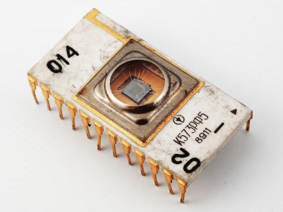
 As a result of scientific-technical progress increases the degree of integration of integrated circuits (MS), including working in a permanent storage device (ROM). The developers of the micro-computer it is possible to use MS’s permanent memory with a larger capacity, thereby increasing the reliability of the computer while decreasing its size and power consumption. However, Amateur radio operators (especially in remote rural areas), this progress is often not happy. The reason is simple: cutting-edge MS from them or not at all, or they are, but beyond available to the programmer.
Last depressing most. Because superintegrable chip with UV Erasure may in five years (and if the window is not closed, even in a year) to lose the stored information due to self-discharge of the gate of the transistor. And not to risk, have once a year by a programmer to restore the former charge or even replace MS itself. Otherwise jeopardizing the ability of the computer repair (no place to find unbiased information).
To verify the correctness of the information recorded in the ROM, you need to check its checksum. This function tests the ZX-SPECTRUM, programs which are listed in a separate chip. Test MS installed the ROM chips of a computer. However, if the latter is disabled, it will not be checked. The test result will only indicate an error checksum ROM.
If ROM are chips with a capacity of 2 Kbytes, then the test will verify the checksum of each MS, except the first, instead of which included a test. The test chip can not be removed and incorporate a toggle switch.
The most important advantage of such a partitioning ROM part with a capacity of 2 KB is that it is possible to use the available MS burn bridges, in which information is not distorted with time and it does not need to periodically restore. If you purchased the fee of small size, designed for the use of ROM circuits of large capacity, the resulting task — posting seventeen cheap MS with a capacity of 2 Kbytes each is solved simply. In particular, MS can be soldered in parallel in a stack one above the other. If some of the chips will burn out (to indicate that constantly included the test all at once to burn can’t), then the dial on the programmer information with a capacity of 2 Kbytes, with only a paper printout, not too difficult (it’s not 8 KB!).
In addition, when there is free space in the ROM of the computer, you receive the possibility of saving MILLISECONDS. An illustration of this is a circuit diagram of the enable circuits with a capacity of 2 KB for the ZX-SPECTRUM. Not 17 MS it is possible to apply, and only 15 (steam saving) with the SOS (DD3—DD10) of the computer TRDOS (DD12—DD17) floppy drive controller and test (DD11). It uses only one decoder on the chip DD1 К555ИД4.
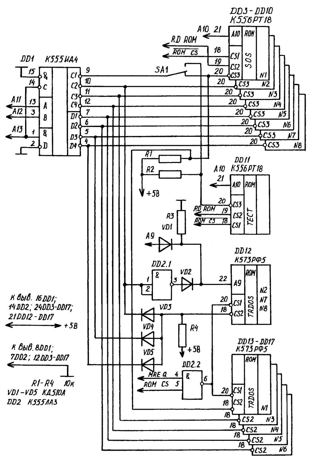
Circuit diagram replace the MS ROM in the microcomputer, for example, ZX-SPECTRUM
Address space the programs SOS and TRDOS, divided into eight “riwnodennyk” areas N1—N8 is 2 KB. Each area is listed in a separate chip, with the exception of the N2, N7, N8 TRDOS, which had managed to put in a DD12 with empty seats. For this we used the decoder on the elements VD1—VD5, DD2.1, R3, R4, resulting in a simple construction, pripal diodes and resistors directly to the pins of the ICS ROM. As example for SOS TEST and used the chip К556РТ18, and for TRDOS — К573РФ5 as more reliable compared to К573РФ6, which halved the number of allowable write cycles and two times shorter than the retention time. There win and when the computer repair: К573РФ5 easier to write information than К573РФ6.
Using the computer and the drive controller in two К573РФ6 the first MS shall work with zero level of address bus A13 processor, and the second with a single. Similar is the case in the above diagram: zero level A13 includes a decoder With DD1, connected with circuits N1—N4, and a single level of A13 decoder D already called MS, coupled with chips, N5—N8.
Just as the MS ROM in the computer are selected in the presence of a signal RDROM (read ROM) and no signal ROMCS (option ROM floppy drive controller) and the following diagram these signals start at the inputs 18, 19 of the selection of crystal chips DD3 — DD11. In the absence of the drive controller is ROMCS is supplied with +5 V.
The ROM chips of the drive controller selects another signal MREQ (memory reading), ROMCS. In the scheme — similarly, the aforementioned signals are got on the entrances of the element DD2.2, the output of which is connected to terminals 20 crystal selection circuits DD12—DD17. Also for chips SOS DD3—DD11: can use the element And opened at its inputs signals RDROM and inverse ROMCS if MS just used two inputs of the selection of crystal, one of which involved a decoder (when used К573РФ5).
With the switch SA1 can be disconnected from the decoder circuits N1 and to connect the MS test. This will check the checksum information of the areas SOS N2—N8.
For TRDOS Ver5.04s in the area of N8 was clean addresses from 000H to 400N, i.e. those that are active in the field N7 (000Н to 1FDH). Therefore, if the region TRDOS N7 and N8 will be recorded in a single chip, then overlay one on the other will not happen, as the region is different ‘ this MS. The signals from decoder DD1 choosing region N7 and N8, you need to apply to the input crystal selection combined circuits DD12 through the element OR performed on the diodes VD4 and VD5.
That is, the DD12 is selected when the processor is areas N7 and N8. For example, if you select a region N8, the CPU does not go to ‘the joint of the chip occupied by the region N7, as in the field of N8 these’ clean. Also, when choosing a region N7 CPU does not go to ‘ the joint of a chip occupied area N8.
Area N2 is almost all clean (except for the 5 bytes at the beginning, but these ‘ busy and DD12). If the selection processor region N2 to proinvestirovatj address signal A9 chip combined, this area can add to the DD12 to the addresses that it is free, since 200N.
The flow of the inverse of the A9 carries the element DD2.1 via the decoupling diode VD2 only during the selection processor region N2. When choosing TRDOS N7 and N8, are included in the merged chip DD12, the input of the A9 will do a normal address signal through the diode VD1.
You can enter the area N2 in the chip DD12 and other locations, Pro-investirovav to this other address bus — one or more. It is also quite valid, not saving IC, each region TRDOS N1—N8 recorded in a separate MS. Need additional decoder then there will be, and all eight chips can be enabled similarly DD3—DD10.
Similar savings MS, you can get at any computer where space is available. ‘These places need to record on paper, so it immediately became clear how to combine information in a single chip and make a decoder for the example above.
The increase in the number of MS ROM virtually no complicated designs of computer, for there is no need for an additional PC Board to mount them and decoder. With DD1, DD2 can be mounted on any of microchip computer (geometrically parallel to it), using two short sections of thick copper wire, soldered to the power pins of the lower and upper MC. These wires will stay and additional circuitry.
Instead each К573РФ6 you can use a stack of four MS with a capacity of 2 Kbytes, it is Advisable to place these MS so that their corps were one above the other, with millimeter clearance for cooling. Same conclusions to solder the wire passing through the entire stack of chips and beyond the bottom body — for inclusion in the socket К573РФ6. An exception is made only for “legs”, which have to be connected to the decoder DD1 and for those that, in accordance with the scheme and the table must not be in nest sockets (they shorten pliers or side cutters and the remaining empty socket sealed with tape to prevent accidental electrical contacts). These combined and shortened leads compiled from the leads of the chips are connected with PCB PC mounting wires and soldering.
Now on the table. It gives the pin numbers and their names (functions) to model К573РФ6 (as on the chip, that is, in ascending order of the numbers in the left column from top to bottom, and the right from the bottom up, it’s as if the chip lies in the middle of the table). Information about “legs” that replaces the MS, corresponding to the findings reported in table columns to the left (for left side) and on the right side (right side chip).
From the table it is seen that a stack of four К573РФ5 can be fully installed in place К573РФ6. It is only necessary to displace the two output back to the first terminal of the chip has entered the third socket the socket. However, only pins 21 and 24 of the chip К573РФ5, which should be supplied voltage +5 V must not fall into located near the contact openings. Mounting wire need to connect these pins with the socket 28 socket exactly as it do when you turn on the test chip during setup of the computer. Must not fall into the socket and the socket terminal 18, which are connected mounting wires soldered to the decoder.
Pin number and function
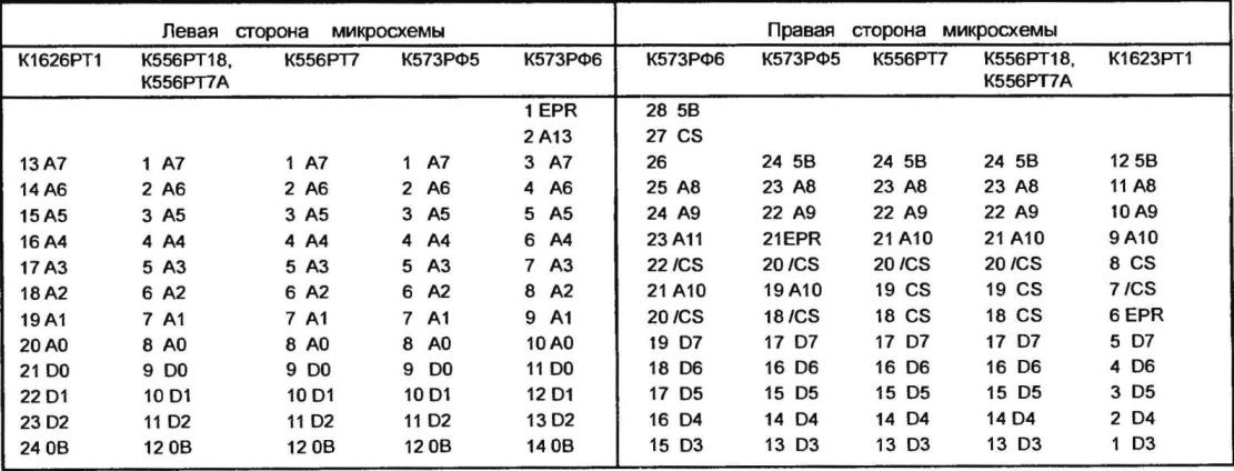
Also have to slip on two pins on back and other chips. In addition, stack MS К1623РТ1 must be installed in the socket backwards (that is, its first conclusion must match the socket 15 socket). If the MS does not coincide with the socket address output a10, it needs to be shortened with wire cutters or side cutters (to prevent accidental connection with the contact socket opposite) and using wire to solder to the point of installation of the computer (where the signal is present a10). With the corresponding same socket the socket this wire to connect inconvenient because it is located above the other conclusions of the stack of chips. Should exclude conclusions MS series К556, К1623 (which is a chip selection CS) into the slot 21 where filed a10.
Inverse inputs CS of the selection of MS should be connected to the decoder DD1 or DD2.2, a direct fed signals RDROM and /ROMCS or MREQ and ROMCS. Conclusion 6 К1623РТ1 must be connected to the common wire, as it is energized during the programming. As for +5 V, it must arrive at conclusions. 24 IC series К556 and conclusions. 12 chip series К1623 directly from the bus power supply.
Wire connectors any inconvenience in the installation and extraction of MS do not have; they are not only easy to solder when the need arises, but also to dismantle. Acceptable even to remove the chip from the socket without additional tap. To consolidate (i.e., record in MS already made) information can also without dismantling the whole stack РФ5: it is only connected to the programmer with supply +5 V To the pins 21 only non-programmable chips. The conclusion is programmable from 21 MS to be connected to the programmer.
Read the programming information you need to close the outputs of all chips of the stack (except read) by feeding the log 1 in their conclusions of 18 or 20 and the terminal 18 and 20 read the chip to connect to the programmer. The conclusions, to which is supplied +5 V or log. 1, must be disconnected from the programmer.
Insights in the selection table MS and open outputs are marked the same way: as the choice of the crystal CS (for this use they are identical and equally affect the outputs of the chips). Chip К556РТ7 and К556РТ7А read the same way, but the programming algorithm is different.
The table used the following symbols: A — ‘(for example, 23 A8 — 23 output 8 drain’), data (say, 9 00 — 9 output a zero bit of data), SB — chip select, the EP TO — output voltage programming 5V supply voltage, + / — sign inversion. First, the number of the output, and then its function.
SOLONIN, Konotop, Ukraine

