
 In 1907, English engineer Round, who worked at the world famous Marconi laboratory, accidentally noticed that running the detector around a point of contact there is a glow. Also seriously interested in this physical phenomenon and tried to find the practical application of “inconceivably talented Russian” — Oleg Vladimirovich Losev.
Found in 1922 during their nightly radioact glow of the crystal detector, this then 18-year-old, ham radio was not limited to the statement “strange” fact, and immediately moved to the original experiments. In an effort to obtain a stable generation of the crystal, it passes through a point contact diode detector current from the batteries. That is dealt with nothing else, like a prototype semiconductor device, later called led. The whole world started talking about “Losev effect” on the practical application which the inventor had to (before his death in the war in 1942), four (!) patent.
Since 1951, the center for the development of “semiconductor lamps”, operating on the basis of “Losev effect” has moved to America, where it was headed by K. Lehovec (USA). In the study of problems associated with LEDs, and took an active part and “father of transistors” physicist W. Shockley.
It soon became clear that germanium (Ge) and silicon (Si), on the basis of which to make a semiconductor triode, hopeless for the LEDs because of too much “work output” and, accordingly, weak emission of photons on p-n junction (more about this in the journal “modelist-Konstruktor” No. 5 and 6 for 1996). The success accompanied the single crystals of complex composite semiconductors — compounds of gallium (Ga), Arsenicum (arsenic — As), phosphorus (P), indium (In), aluminum (Al), other elements of the periodic system. As a result, in the late 60-ies LEDs, becoming quite technologically advanced devices with stable parameters, began to increasingly enter our daily life.
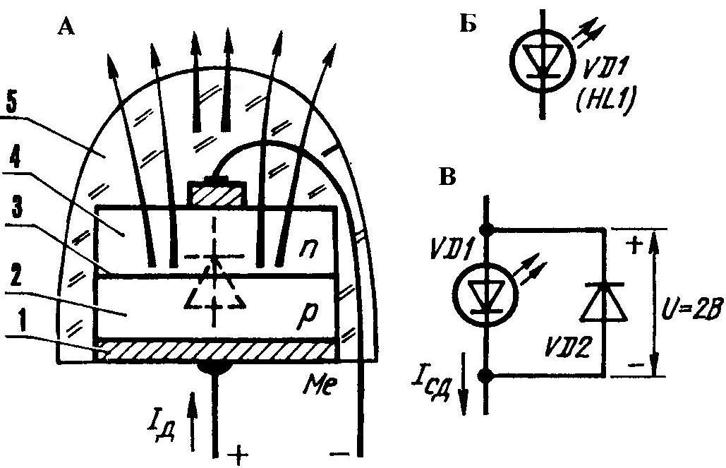
Standard LEDs (A) conventional image (B) and surge protection parallel connection of a semiconductor diode in the “reverse” direction (In):
1 — ohmic contact (2); 2 — p-the area of the active element (chip) of semiconductor material; 3 — p-n junction; 4 — n-region of chip; 5 — lens
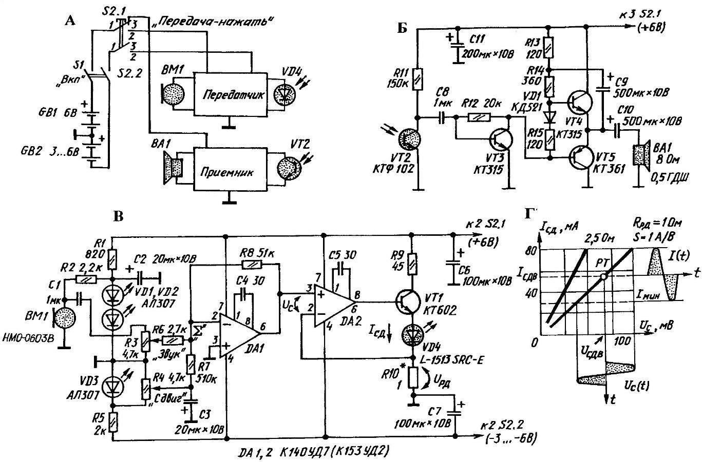
Structural diagram homemade sweetelena (A), schematics of the transmitter (B) family of output characteristics (Y) and the receiver (In)
In the cross section of a crystal of any of the modern LEDs can be divided into two region: p-and n-conductivity. Led light is the result of recombination (connection) of electrons and holes on the surface of the p-n junction during the occurrence of a strong direct current (“Losev effect”). Minority carriers (for the recombination process is the electrons) come into the p region of the led from the electrical power source. The more current in the “forward” direction PR, the more comes electrons and the stronger the flow of light emitted from the surface of the p-n junction.
As for the brightness, then it is not indifferent and optical clarity n-region (ultrathin films of semiconductors are quite transparent). Well, the color (frequency) of radiation, having a clear functional relationship with the energy of the emitted photons depends on the semiconductor materials p-n junctions. In particular, a pure monocrystal of GaAs gives the infrared beam, a small additive of Al and/or P changes the emission color to red. The green light emitting GaP. The use of p-n junction on the basis of the composition allows to obtain dual color mini-yellow or orange light. Blue LEDs were late for twenty years — used components of a complex and even now are very expensive. Well, the LEDs are white (the real “semiconductor light bulbs”), there are still only in draft.
The active element is a semiconductor monocrystal in most modern LEDs used in the form of a die (chip) size 0,3×0,3×0,25 mm, containing the p-n or heterojunction and ohmic contacts. However, LEDs are also available with two chips (in different color of light) or one, but having a pair of p-n junctions that emit in two spectral bands. In this case you can control the glow color. There are more complex structures with embedded electronic components or chip, which allows to control the supply voltage. Very often all combined in a transparent plastic casing (with the cap in the form of microlenses or contain other elements concentration of radiation, enhancing the exterior of the optical efficiency and the necessary orientation of the radiation).
All gallium arsenide LEDs have similar electrical parameters. For these semiconductor devices characterized by a sufficiently large direct (forward) voltage drop Ypres = 1,8…2,2 V. But, unfortunately, a valid reverse (breakdown) voltage Uo6p also is a few volts. And it is necessary to consider protecting the LEDs from dangerous overvoltage additional input silicon diode in the “reverse” is turned on.
As a rule, led working indicator, it is enough 1-2 mA. Well, where is required high brightness of illumination (concentrated, say, in a narrow beam) use a special semiconductor (including a laser!) devices or increase the current a standard led with a built-in winsocki, not forgetting the observance of the thermal mode. When SD equal to, for example, 50 mA, the led average brightness will dissipate about 100 mW. And the cost of radiation are only a few mW, the remaining power necessary from the led can take without overheating the crystal.
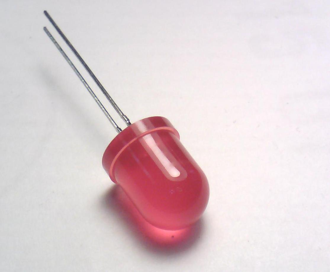
From the first LEDs were able to light force not exceeding a few tens of microchannel (candela candle). It’s not a deficit, even super-bright LEDs, which is a 3.5 KD is not the limit. Based on the use is quite common semiconductor devices are designed, in particular, and original homemade sweetlife. Using two of these devices are easy to organize, for example, a private light connection, the type of industrial laser.
Analysis the circuit diagram of the transmitting channel sweetelena better to start with a light emitter VD4 — a relatively inexpensive led L-1513SRC-E, manufactured by Knightbright. This led of 5 mm diameter is able to create directional red light with a light intensity of 3.5 CD. Its linear modulator brightness is performed on the operational amplifier OPAMP of the type К140УД7 (К153УД2). Moreover, in the embodiment of the structure imposed on the readers loved the magazine, this “operazioni” works as a voltage Converter of the signal Uc to the load current IR equal to SD of the light emitter.
Indeed, for the high quality of OU control voltage observed between the inputs, can be considered zero. This means that the voltage drop across the resistor-sensor RD (R10) when the flow of the load current must be almost equal to the signal voltage, that is, Uc = Upд = lсдRpд. It is easy to calculate the current flowing through the led: SD = Uc/Rрд. The steepness of amplification of the cascade, respectively, will be S = I/Is = 1/Rрд.
Family typical performance characteristics led L-1513SRC-E can be found and the optimal power mode VD4 light emitter current SD. When Rрд about 1 Ohm (that is the nominal value of R10 from the circuit) the steepness of the S will be 1 A/V. the resistor-current limit R9 is 45 Ohms, minimum (threshold) current Min = 30 mA, maximum current Imax = 80 mA. The working point RT is selected in the middle of the linear section of the graph. To enable this mode on the+input of op-amp DA2 was required to file a potential shift of Uсдв = 55 mV overlay on it signal with amplitude Uc(t) = ±25 mV. And since the output current OPAMP for General use may not exceed 25 mA, the feedback loop added current amplifier — medium power transistor VT1.
To +what considered Oh to form the desired signal with the required capacity of the shear used of the summing inverting amplifier DA1. Moreover, it is made so that at the point Sigma was met two current: R6 — lc(t) “Sound”, and through resistor R7 — tсдв “Shift”.
The sign is negative, these currents are fed to the input of the DA1. Flowing through the feedback resistor R8, they will give +DA2 desired composition of Uсдв and Uc(t) of positive polarity.
Chain R1-VD1-VD2-VD3-R5 — is a source of auxiliary potential and current needed for proper operation of the circuit in which LEDs are used as a good low voltage Zener diodes to 1.8 V. In particular, the diode VD3 via potentiometer R4 taken -0.5 In to direct to the point “Sigma” for the current shift. The diodes VD1 and VD2 are capable to provide the supply voltage 3.6 V “electretic” (a variant of the condenser microphone with integrated field-effect transistor) ВМ1 type NMO-0603В. After all, this highly sensitive transducer sound waves into electrical — minimum power consumption (supply current of about 0.5 mA). The amplitude of the same sound current coming from the electret microphone to the point of “Sigma”, can be adjusted by resistor R3.
Under a and a circuit diagram of the receiving channel sweetelena. A photodetector of the modulated red beam is the phototransistor VT2 type КТФ102 with the load R11. Transistors VT3 — VT5 and related parts constitute the simple scheme of ULF with an output of approximately 100 mW. Speaker BA1 — any type (as long as it was 8-Ohm and small). Capacitor C9 operates in the input circuit of the transistors VT4 and VT5. In foreign literature demonstrated here the effect of cross-feedback, are figuratively referred to as “bootstrapping,” which is sometimes translated as “lacing Shoe”.
Manufacturer svetotehnika apparatus in the home workshop — it although time-consuming, but it is quite feasible, even for novice hams. The most complicated installation of the optic-mechanical block (OMB), to cope with which will help technology, published in the journal “modelist-Konstruktor” No. 10’98 (p. 17).
Of course, the dimensions and features of installation of POM depends largely on the lens. Preferably short throw, without adjustment for distance (as in photo-devices-point-and-shoots). Given that sweetelena bilateral context, requires two transmitter / receiver apparatus, must be purchased for them two lens. In the same way as super-bright LEDs L-1513SRC-E, phototransistors КТФ102, the other two used semiconductor devices.
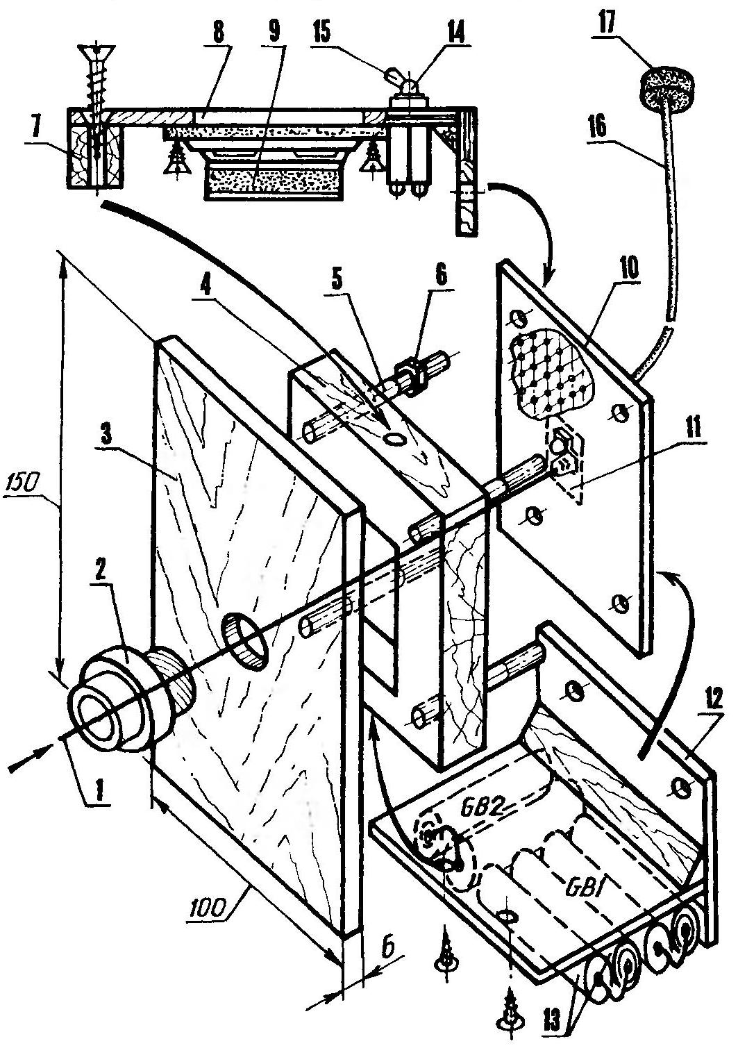
Optical-mechanical unit:
1 — a ray on the optical axis; 2 — lens; 3 — front panel; 4 — the supporting frame; 5 — stud M4 (4 PCs); 6 — nut M4 (8 pieces); 7 — mounting bar; 8 — upper panel; 9 — speaker; 10 — mounting plate with holes; 11 — Central site installation (with a super bright led and a phototransistor); 12 — lower panel; 13 — power supply 1.5 V; 14 — button “Transfer-push”; 15 — the toggle switch “On.”; 16 — flexible microphone shielded cord; 17 — electret microphone
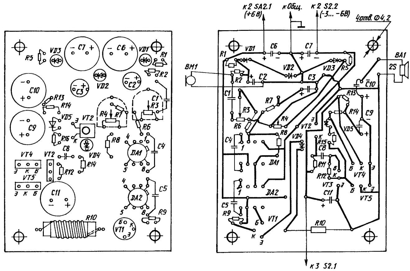
Circuit Board from the electronic components and soldering
Making OMB, the light emitter and the photodetector should be placed in the center of the circuit Board. But so that their crystals being in the focal plane of the lens was located as close as possible to the optical axis (that is, occupied the center of the frame). And to tie the whole structure and positioning of “tele” position of the Board is necessary to provide to OMB by four studs M4 with the adjustment nuts. The very same focusing optics recommended tightly, just like a screw, to screw in a neat (performed under the thread diameter on the lens) hole on the front wooden panel.
An important detail of OMB — supporting frame. It should be cut from oak or beech piece and attach with glue “88” to the rear side of the front panel. Under studs M4 (the length of each of them should double the focal length of the lens) to make the appropriate threaded holes M4. Screw on glue “88” in a frame all uprights, to put the circuit Board and fix the inner and outer nuts. Then go to the top node overhead panel with a speaker, a power switch S1 “On” S2 button and the “Transfer press”.
Power supply sources are arranged in a plywood “basement” mount which is similar to fastening the top surface of the node. Galvanic cells connected in the battery soldered (like is done in development, published in the journal “modelist-Konstruktor” No. 10 of 1998).
Given that the “zero setepolotna” battery consumption is faster than “minus Travolta” — it’s the nature of homemade sweetelena, it is recommended that (especially in energy-intensive adjustment of the device) to use a lab power supply +6 V is provided with a milliammeter on the 100 mA. And electric installation, configuration of the transmitter and receiver at the stage of debugging and experimentation is best done step-by-step on two sets: first, incomplete (one-sided), and then (for two-way communication).
In any case, it will be parallel work on two devices for which it is necessary to have a circuit Board the size 90x70x1,5 mm of non-foiled textolite or any solid sheet of electrical insulator, down to the cardboard. In two boards at once, temporarily “taking” the glue “Moment”, it is necessary to drill a grid of holes (drill with a diameter of 0.9 mm with a step of 2.5 mm). Marking with a Scriber (20 columns and, respectively, 30 rows). Drilling is better at low speed drills, undermining from time to time a diamond needle file cutting edges of microsphere. In addition, drilled four holes for the passage of the rack-pins M4.
As mentioned earlier, the light emitter and the phototransistor should be placed in the center of each of the boards, between the holes in the pin and as close as possible to each other. Further makes sense on one half of Board # 1 is to mount the radiation receiver. It should work immediately, if assembled correctly and of serviceable electronic components.
For connection to a power source speaker such a receiver will respond to a slight noise. Well, if you install a mounted charge OMB No. 1 and to direct his lens on the screen the TV works, from the same dynamics you will hear a “roar” of vertical sweep. Moreover, the presence of such a stable signal will allow, if necessary, to readjust and the ULF.
Complete electrical installation of sleeperette for “unilateral command of the” sweetelena (as the initial works on bilateral ties) is on the Board № 2. Moreover, the Assembly and testing it is recommended to parascale. Progress is fast, if no mistakes are made and used reliable parts.
Feeding the first low (3) “bipolar” power, are closely watching the testimony of laboratory milliammeter. Make sure that current consumption is “normal”. Then Usup is increased to 6 V and the resistance change of the variable resistor “Shift” after the extinction of the light emitter (engine at the top of the scheme) or, conversely, increase its brightness (engine down), preventing the current consumption exceeded 60 mA. The variable resistor “Sound” adjusts the depth of modulation, focusing on more or less the flickering beam.
After the installation of sleeperette in OMB № 2 begin experiments on one-sided “team” connection. “Aim” through two lenses to get the beam from the transmitter No. 2, the phototransistor of the receiver No. 1 is not so easy. The relationship of the experimental to the same gun! However, implementation of the settings (and during operation) must not be allowed to super-bright beam even for a moment fall into the eyes. Especially more powerful than in the development of hoteislakitira.
Having sound feedback from the device No. 1, regulate the quality of the effect-variable resistors “Shift” and “Sound” of the device No. 2. Then proceed to the installation of receiver No. 2 and the transmitter No. 1. The result is a two-way channel sweetelena of communication where the receivers are permanently enabled state. Any of the light emitters while in standby mode, is activated as needed: click the “Gear-click” on the appropriate apparatus. Simultaneously disconnected from the electrical power source located with him on a single Board receiver. Toggle “On” to turn on / off the device.
V. AWL, radio engineer
Recommend to read
 POCKET GRILL
The design of this portable barbecue grill is convenient to use in field conditions (e.g., hikers, hunters or fishermen), and in the garden area or in the country for quick cooking... Garden “fire pit”
Shashlik has long been a cross-national (or cross-regional) dish, spreading across the former USSR and beyond. Every enthusiast has their own “signature” secret for making it. Many now...
